Inline (Inline Metrology and Inspection)
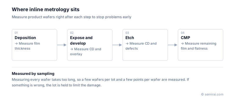
Inline, in semiconductor manufacturing, describes work done inside the production line while product wafers keep flowing. Inline metrology and inspection measure film thickness, critical dimension, overlay and defects on product wafers right after key process steps, so that a drifting tool is stopped before many more wafers are affected.
Also called: in-line, inline metrology, inline inspection
Diagram
Inline, offline and in-situ
Three terms describe where a measurement happens. In-situ measurement takes place inside the process tool during processing. Inline measurement takes place on dedicated metrology and inspection tools within the line, after a step is finished. Offline analysis removes wafers from the line and examines them in a laboratory with methods such as cross-section TEM or SIMS, which are detailed but slow and often destroy the wafer.
A chip passes through hundreds of steps over weeks or months. If a problem were found only at the final electrical test, every wafer processed in the meantime could be lost. Inline results therefore feed statistical process control, which holds lots and tools when limits are crossed, and advanced process control, which corrects settings for the next lot.
Sampling and its trade-offs
Measuring every wafer at every point would need many more tools and add cycle time. Fabs therefore sample: a few wafers from each lot and a set of points on each wafer, with more sampling at critical layers. Virtual metrology models estimate the results of unmeasured wafers from tool data to fill the gaps.
Inline as a tool configuration
Inline also describes tools that are physically linked. A coater/developer track is connected inline to a lithography scanner, so resist coating, exposure, post-exposure bake and development run without wafers leaving the system. This keeps the delay before baking constant, which matters for the line-width control of chemically amplified resists. Inline sputtering systems, in which substrates move in one direction through a row of chambers, use the word in the same sense.
Japanese companies involved
- Hitachi High-Tech makes CD-SEMs and wafer inspection systems that are installed inline in many fabs.
- Lasertec makes optical inspection systems and is best known for EUV mask and mask blank inspection.
- Hitachi High-Tech · CD-SEM metrology, defect inspection and etch systems
- Lasertec · EUV mask and mask blank inspection
FAQ
Is inline metrology destructive?
No. Inline tools are chosen so that product wafers can continue through the line after measurement. Methods that cut or consume the wafer, such as cross-sectioning or SIMS, are done offline on test or sacrificial wafers.
What is a monitor wafer?
A monitor wafer is a bare or simply processed wafer run through a tool to check its condition, for example particles added or film thickness deposited. It is cheaper to measure than product, but it does not show how the tool behaves on real patterns, so fabs use both.
Related pages
Sources
Last updated: November 2, 2026