Yield
Yield is the fraction of manufactured units that meet specification. In semiconductor manufacturing it most often means die yield: the number of good chips on a wafer divided by the total number of chips on it. Because a wafer costs roughly the same however many of its chips work, yield sets the cost of each good chip.
Also called: die yield, wafer yield, manufacturing yield
Diagram
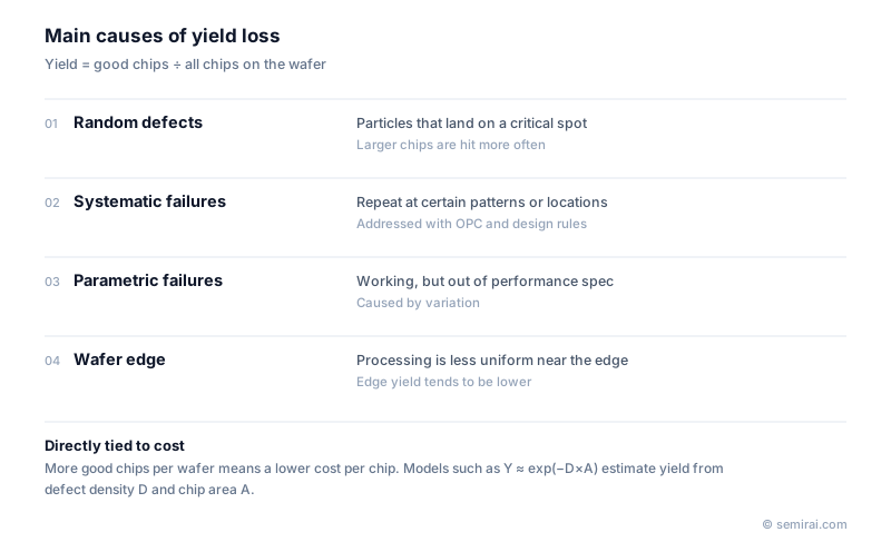
What lowers yield
Random defects, such as particles, land on the wafer by chance and kill a chip only if they fall on a sensitive spot. Systematic defects repeat at particular layout patterns or wafer locations because of how the design interacts with lithography, etch or CMP. Parametric failures are chips that are not broken but miss a speed, leakage or power target because of process variation. Yield is also typically lower near the wafer edge, where processing is less uniform.
Fabs track several yields: line yield (wafers that survive processing), die yield at wafer sort, and final test yield after packaging. Multiplying them gives the overall figure.
Yield models
The simplest model is the Poisson model, Y ≈ exp(−D×A), where D is the density of killer defects and A is the chip area. Defects tend to cluster, so the Murphy and negative binomial models give more realistic numbers. Refinements use the critical area, the part of the layout where a defect of a given size would actually cause a failure.
All models share one lesson: for a given defect density, larger chips yield worse. This is one reason designers split very large systems into several smaller chiplets.
How yield is improved
Yield enhancement combines defect inspection and review to find and remove defect sources, process control to reduce variation, design for manufacturability (DFM) to avoid layouts that print badly, and contamination control in the cleanroom. New process nodes start with lower yield and are improved over a ramp that can take many months.
Japanese companies involved
- Hitachi High-Tech makes defect inspection, defect review SEM and CD-SEM systems that fabs use to locate yield-limiting defects and variation.
- Hitachi High-Tech · CD-SEM metrology, defect inspection and etch systems
FAQ
Why do large chips cost disproportionately more?
A larger chip both fits fewer times on a wafer and is more likely to contain a killer defect. The two effects multiply, so the cost per good chip rises faster than the area.
Can a chip with a defect still be sold?
Sometimes. Memory chips include spare rows and columns that can replace defective ones, and processors may be sold with a faulty core or cache block disabled. These repair and binning methods raise effective yield.
Related pages
Sources
Last updated: November 2, 2026