Atomic Layer Etching (ALE)
Atomic layer etching (ALE) is a technique that removes material in a self-limiting way, about one atomic layer per cycle. Each cycle first modifies only the topmost layer of the surface and then removes only that modified layer. It is the removal counterpart of atomic layer deposition (ALD) and gives depth control and selectivity that continuous plasma etching cannot match.
Also called: ALE, atomic-layer etch
Diagram
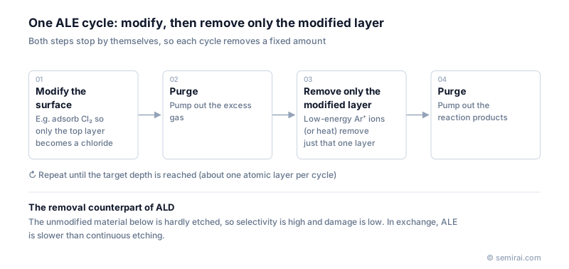
How an ALE cycle works
In plasma ALE of silicon, for example, chlorine is first adsorbed so that only the surface layer becomes a chloride. After the excess gas is purged, low-energy argon ions strike the surface with just enough energy to remove the chlorinated layer but not the unmodified material below. A second purge pumps away the products, and the cycle repeats until the target depth is reached.
Because both steps stop by themselves, the amount removed per cycle is fixed by chemistry rather than by time, which makes the process insensitive to small variations in dose or uniformity across the wafer.
Plasma ALE and thermal ALE
Plasma ALE uses directional ions in the removal step, so it etches mainly downward. Thermal ALE uses only surface chemistry and heat, with no plasma, so it removes material evenly in all directions. That isotropic behaviour suits lateral recesses in three-dimensional structures and delicate materials that ions would damage.
ALE is applied where a few nanometres matter: gate spacer and gate recess steps in FinFET and gate-all-around transistors, thin metal and high-k film removal, and fine trimming of patterns.
Strengths and limits
Compared with conventional reactive ion etching, ALE offers atomic-scale depth control, high selectivity to neighbouring materials and low surface damage. Its weakness is speed: each cycle takes seconds and removes only a fraction of a nanometre, so it is used selectively on critical steps, often combined with faster continuous etching.
Japanese companies involved
- Tokyo Electron (TEL) develops atomic layer etching processes for its etch systems, as do the US equipment makers Lam Research and Applied Materials.
- Tokyo Electron (TEL) · Coat/develop, etch and deposition equipment
FAQ
How is ALE related to ALD?
Both split a process into two self-limiting half-reactions separated by purges. ALD adds about one atomic layer per cycle, while ALE removes about one. Some research uses the two together to deposit and trim films with atomic precision.
Why is ALE more selective than normal etching?
The removal step uses ions with too little energy to sputter unmodified material. Only the chemically modified layer comes off, so an underlying film of a different material that the first step does not modify is barely touched.
Comparisons
Related pages
Sources
Last updated: November 2, 2026