Package Substrate
A package substrate is the small multilayer wiring board that sits between a semiconductor die and the printed circuit board. It fans out the die's fine-pitch terminals to the much coarser pitch of the solder balls below, distributes power and ground, and gives the package its mechanical base.
Also called: IC substrate, IC package substrate
Diagram
Materials and structure
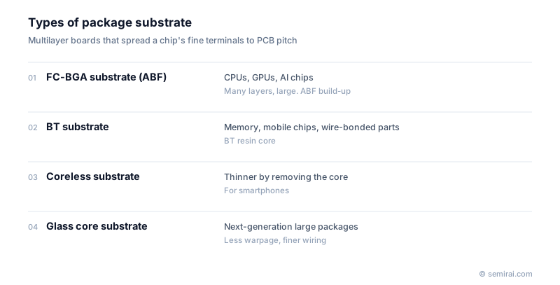
A substrate consists of a core with insulating layers and copper wiring built up on both sides and connected by microvias. Two resin systems dominate. BT (bismaleimide triazine) resin substrates are used for memory, mobile chips and many wire-bonded packages. For high-end flip-chip BGA (FC-BGA) packages, the build-up layers are made from ABF (Ajinomoto Build-up Film), a film material that can be laser-drilled and plated with very fine lines.
Processors for servers and AI need large substrates with many build-up layers and line widths and spaces of only a few micrometres, formed by semi-additive processes. Larger and thinner substrates are harder to make flat and defect-free, so yield and capacity are constant concerns. Coreless substrates, which remove the core to make the package thinner, are used in some mobile products.
Warpage and the move to glass
In 2.5D packages, a silicon interposer and several dies sit on a large organic substrate. Silicon and organic materials expand by different amounts when heated, so the assembly warps during reflow and operation. Controlling this warpage is one of the main limits on package size.
Glass core substrates are being developed as a next step. Glass is flatter and more dimensionally stable than organic cores and its expansion can be tuned closer to silicon, which allows finer wiring and larger packages. Intel and several substrate makers have announced development programmes, but glass cores are not yet in high-volume production.
Japanese companies involved
- IBIDEN, Shinko Electric Industries and Kyocera make FC-BGA and other package substrates for processor and memory makers.
- Ajinomoto developed and supplies ABF, the insulating film used for the build-up layers of high-end substrates.
- IBIDEN · IC package substrates (FC-BGA)
- Shinko Electric Industries · FC-BGA package substrates and lead frames
- Ajinomoto · ABF insulating film for package substrates
- Kyocera · Package substrates and ceramic components
FAQ
What is the difference between a package substrate and a PCB?
Both are wiring boards, but a package substrate is much smaller and has far finer lines and vias, measured in micrometres rather than tenths of a millimetre. It connects one chip to the PCB, while the PCB connects many packages to one another.
Why are ABF substrates often in short supply?
High-end processors need large substrates with many layers, and each extra layer and each increase in size lowers yield. Adding capacity requires new factories and long qualification, so demand surges, such as those from AI servers, can outpace supply.
Related pages
Sources
Last updated: November 2, 2026