Microloading Effect
The microloading effect is a dry etching phenomenon in which the etch rate varies locally with pattern density and opening size. Even on the same wafer under the same conditions, dense and sparse areas, or wide and narrow openings, etch to different depths. It is called micro loading to distinguish it from macro loading, where the total exposed area of the whole wafer changes the etch rate.
Also called: microloading, pattern density effect
Diagram
Why it happens
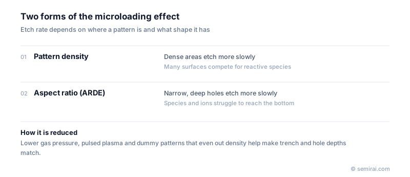
The cause lies in how reactive species are consumed and transported locally. Where openings are packed closely, many surfaces consume radicals at the same time, so the local supply runs short and etching slows. In narrow, deep holes and trenches, radicals and ions have difficulty reaching the bottom and reaction products have difficulty escaping, so the rate falls as the aspect ratio rises.
Strictly, this second effect is called RIE lag or aspect-ratio-dependent etching (ARDE), but it is often included in microloading in the broad sense. Under some conditions the reverse happens and narrow openings etch faster, which is called inverse microloading.
Why it is a problem and how it is reduced
Trenches and contact holes that should all reach the same depth end up underetched in some places and overetched in others. Adding more overetch to clear the slow areas attacks the underlying layer where the etch finished first, so the two goals conflict.
Countermeasures include lowering the pressure to improve transport of reactive species, pulsing the plasma to give reaction products time to leave, alternating etch and passivation steps, and adding dummy patterns at the design stage so that pattern density is more even. The effect is especially important in high-aspect-ratio etching such as the deep memory holes of 3D NAND.
Japanese companies involved
- Tokyo Electron (TEL) and Hitachi High-Tech, both makers of plasma etch systems, address microloading through chamber design and process conditions such as pulsed plasma and gas flow control.
- Tokyo Electron (TEL) · Coat/develop, etch and deposition equipment
- Hitachi High-Tech · CD-SEM metrology, defect inspection and etch systems
FAQ
What is the difference between microloading and RIE lag?
In the strict sense, microloading refers to rate differences caused by pattern density, while RIE lag (ARDE) refers to differences caused by the width and depth of individual openings. In practice the two appear together, and many engineers call both microloading.
Can design rules help?
Yes. Chip designers are often required to keep local pattern density within a set range, and empty areas are filled with dummy features. A more even density reduces local differences in etch rate, just as it reduces thickness variation in CMP.
Related pages
Sources
Last updated: November 13, 2026