X-ray Photoelectron Spectroscopy (XPS)
X-ray photoelectron spectroscopy (XPS) is a surface analysis method that irradiates a sample with X-rays and measures the energy of the electrons emitted from it. It identifies which elements are present in the top few nanometres and in what chemical state they are, for example whether silicon is elemental or oxidised. It is also known as ESCA.
Also called: XPS, ESCA, electron spectroscopy for chemical analysis
Diagram
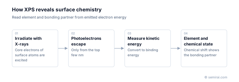
How XPS works
An X-ray photon gives all its energy to a core electron. The electron leaves the atom with a kinetic energy equal to the photon energy minus its binding energy and a small instrument constant. Measuring the kinetic energy therefore gives the binding energy, which is characteristic of each element and core level, so the spectrum identifies the elements present.
Binding energies also move by small amounts depending on what each atom is bonded to. Reading these chemical shifts distinguishes, for instance, silicon in the substrate from silicon in its oxide, or a metal from its nitride. Peak areas, corrected with sensitivity factors, give approximate composition. The measurement is made in ultra-high vacuum so that the electrons reach the analyser.
Why XPS is surface-sensitive
Photoelectrons lose energy in collisions after travelling only a few nanometres through a solid, so only those from near the surface escape with their original energy. This makes XPS ideal for native oxides, the chemical bonds at the interface between gate oxides or high-k films and silicon, and residues left after cleaning or etching.
Alternating measurement with gentle ion sputtering gives a depth profile through thin films. For deeper profiles and trace impurities, secondary ion mass spectrometry (SIMS) is more sensitive; for small spots, electron-beam methods such as Auger spectroscopy offer better lateral resolution.
Japanese companies involved
- ULVAC-PHI makes XPS systems, including scanning microprobe instruments used for semiconductor surface analysis.
- JEOL and Shimadzu also supply XPS instruments; Shimadzu does so through its subsidiary Kratos Analytical.
FAQ
What can XPS not detect?
It cannot detect hydrogen or helium, because they have no core electrons suited to the measurement. Its detection limit is typically around a tenth of an atomic percent, so trace dopants and contaminants need SIMS or TXRF instead.
What is hard X-ray photoelectron spectroscopy (HAXPES)?
HAXPES uses higher-energy X-rays, often at a synchrotron, so photoelectrons leave with more energy and escape from greater depths. It can probe buried interfaces a few tens of nanometres down without sputtering, which avoids damage to the chemical states being measured.
Comparisons
Related pages
- Chemical Shift (XPS)
- Secondary Ion Mass Spectrometry (SIMS)
- X-ray Absorption Near Edge Structure (XANES)
- Energy Dispersive X-ray Spectroscopy (EDX / EDS)
- Native Oxide
- Gate Oxide (Gate Dielectric)
- High-k Dielectric
- Ultra-High Vacuum (UHV)
- Failure analysis equipment
- JEOL HAXIS LIM
- JEOL LazEdge
- Hamamatsu Photonics Dual PHEMOS®-X C16506-01
- Hamamatsu Photonics iPHEMOS®-DDX C18040-11
Sources
Last updated: November 13, 2026