Through Hole
A through hole is a hole that passes through a printed circuit board from front to back, with copper plated on its walls to connect the wiring on the two surfaces and on inner layers. It is often called a plated through hole (PTH). The term also refers to through-hole mounting, in which component leads are inserted into such holes and soldered.
Also called: plated through hole, PTH, through-hole mounting, THT
Diagram
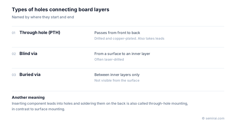
How through holes are made and other via types
The board is drilled, a thin layer of copper is deposited chemically on the hole walls, and electroplating then builds it up to the required thickness.
Besides through holes, there are blind vias, which run from a surface to an inner layer, and buried vias, which connect only inner layers and cannot be seen from outside. In HDI boards and package substrates, small laser-drilled vias are stacked layer by layer, and through holes are used mainly in the core.
Through-hole mounting
In through-hole mounting, the leads of packages such as the DIP are inserted into holes and soldered on the far side, usually by wave soldering. It was the main assembly method before surface mount technology (SMT) spread.
Today SMT dominates because it allows smaller components and denser boards, but through-hole mounting is still used where strength matters: high-current parts, connectors that take repeated plugging forces, and large electrolytic capacitors.
Japanese companies involved
- IBIDEN manufactures package substrates and printed circuit boards, in which plated through holes in the core connect the build-up layers on each side.
- IBIDEN · IC package substrates (FC-BGA)
FAQ
What is the difference between a through hole and a via?
Via is the general term for any hole connecting layers, including blind and buried vias. A through hole is the kind that goes all the way through the board. Holes large enough to take component leads are almost always called through holes.
Why is through-hole mounting still used?
Leads that pass through the board and are soldered on the far side are held much more firmly and can carry large currents. For connectors, heavy capacitors and power components, this mechanical strength is easier to achieve than with surface-mount joints.
Related pages
Sources
Last updated: November 12, 2026