Void (Packaging Defect)
A void is an unintended small cavity, usually filled with gas, inside a semiconductor package. Voids form in mold compound, solder joints, underfill and die attach layers. They block heat and current, concentrate stress and become starting points for cracks and delamination, so void levels are a key quality measure.
Also called: voiding, bubbles, cavity defect
Diagram
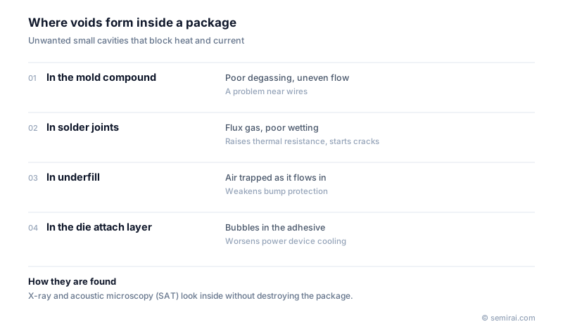
Where voids form and why
In molding, voids come from air that is not vented from the cavity, moisture or volatile substances in the compound, or uneven flow fronts that meet and trap air. In solder joints, gas from evaporating flux or poor wetting leaves bubbles in the solder, especially under large areas such as the thermal pad of a QFN.
Underfill traps air when its flow front moves faster around the edges than through the middle of the gap, or when it passes dense bump arrays. In die attach layers, voids come from trapped air, outgassing during cure or poorly controlled sintering. In power devices the die attach void ratio, the void area as a share of the joint, directly raises thermal resistance and is held to a specified limit.
Detection and prevention
Voids are found without destroying the package by X-ray inspection, including computed tomography (CT), which shows dense materials such as solder, and by scanning acoustic microscopy (SAM or C-SAM), which detects reflections from air gaps and delamination. Cross-sectioning is used in development to confirm what the images show.
Prevention combines materials, equipment and process conditions: vacuum or well-vented molding, compression molding, degassed materials, low-voiding flux, vacuum reflow, optimised heating and curing profiles, and designs that guide flow. As packages become finer and contain more layers, smaller voids matter and inspection needs higher resolution.
FAQ
Are some voids acceptable?
Small voids are often tolerated within limits set by standards or customer specifications, for example a maximum total void area in a solder joint. The acceptable level depends on where the void is: a void under a hot power device is far more harmful than one in a non-critical area.
What is vacuum reflow?
A soldering process in which the chamber is evacuated while the solder is molten, so trapped gas bubbles expand and escape. It is widely used for power modules, where low voiding under the die is essential.
Related pages
Sources
Last updated: November 1, 2026