High-NA EUV Lithography
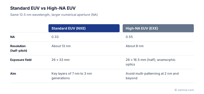
High-NA EUV lithography is the next generation of extreme ultraviolet lithography, raising the numerical aperture (NA) of the projection optics from 0.33 in current EUV scanners to 0.55. It keeps the 13.5 nm wavelength but resolves roughly 1.7 times finer lines, about 8 nm half-pitch, so patterns that would otherwise need EUV multi-patterning can be printed in one exposure.
Also called: High Numerical Aperture EUV, 0.55 NA EUV, EXE
Diagram
What changes in the optics
Collecting light over wider angles requires much larger mirrors. If the projection optics kept the usual 4x reduction in both directions, the light would strike the mask at angles too steep for its multilayer to reflect well. High-NA systems therefore use anamorphic optics: 4x reduction in one direction and 8x in the other.
The consequence is that the exposure field is half the size of a standard field, 26 × 16.5 mm instead of 26 × 33 mm. Chips larger than a half field must be printed in two parts and stitched together, and more fields per wafer mean the stages must move faster to keep throughput up. The optics are made by ZEISS, and ASML's EXE platform is the only High-NA system.
What else has to change
Higher NA reduces depth of focus, since focus depth falls with the square of NA. Wafers, masks and resist films therefore have to be flatter and more uniform. Finer features also mean fewer photons per feature, so stochastic effects such as line edge roughness and random missing or bridging features become harder to control. Thinner resists are needed, which in turn increases interest in metal-oxide resists and new underlayers.
Masks, mask inspection and computational lithography all have to be adapted to the anamorphic imaging. The first High-NA tools went to leading logic makers, Intel first among them, for process development before production use.
Japanese companies involved
- JSR, Tokyo Ohka Kogyo (TOK) and Shin-Etsu Chemical develop resists for EUV, including High-NA EUV; JSR owns Inpria, a developer of metal-oxide resists.
- Lasertec makes actinic mask inspection systems that examine EUV masks with 13.5 nm light.
- Lasertec · EUV mask and mask blank inspection
- JSR · Photoresists and semiconductor materials
- Shin-Etsu Chemical · Silicon wafers, photoresists and photomask blanks
- Tokyo Ohka Kogyo (TOK) · Photoresists and high-purity process chemicals
FAQ
Why not just make the wavelength shorter again?
A shorter wavelength than 13.5 nm would need a new light source, new multilayer mirrors and new resists all at once. Raising NA reuses the EUV source, mask technology and much of the infrastructure, so it is the next practical step.
Will High-NA replace standard EUV?
No. High-NA is expected to be used only for the most critical layers, with 0.33 NA EUV and DUV tools printing the rest. Each tool type is used where its resolution is actually needed, because cost per exposure rises with capability.
What does anamorphic mean here?
The image is reduced by different amounts in the two directions, 4x and 8x. The mask pattern is therefore stretched in one direction compared with the wafer pattern, and design and OPC software must handle the asymmetry.
Comparisons
Related pages
Sources
Last updated: November 2, 2026