Focused Ion Beam (FIB)
A focused ion beam (FIB) system aims a finely focused beam of ions, usually gallium, at a sample to remove material, image it or deposit films at chosen locations with nanometre precision. Ions are far heavier than electrons, so they knock atoms out of the surface. Most systems combine the ion column with an SEM in one instrument, called a FIB-SEM or dual-beam.
Also called: FIB, FIB-SEM, dual-beam, plasma FIB
Diagram
Main uses in semiconductors
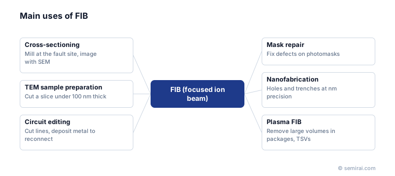
The first use is cross-sectioning. After a failing location has been narrowed down, the FIB mills a trench exactly there and the SEM images the exposed cross-section. The second is preparing samples for transmission electron microscopy (TEM): the FIB cuts out a thin slice, called a lamella, typically less than 100 nm thick, and lifts it out of the chip.
The third is circuit editing. The beam cuts metal lines, and with a precursor gas flowing it deposits metal or insulator to make new connections, so designers can test a fix on real silicon without making new masks. FIB tools are also used to repair defects on photomasks. Serial sectioning, milling slice after slice while imaging each face, builds 3D reconstructions of structures.
Limits and variations
Gallium ions implant into the sample and damage a thin surface layer, which matters for high-resolution TEM. Final polishing with a low-voltage beam reduces this damage. When large volumes must be removed, for example in package cross-sections or through-silicon via (TSV) analysis, plasma FIB tools using xenon ions mill much faster.
In failure analysis, FIB usually follows fault isolation. Methods such as OBIRCH (optical beam induced resistance change) or thermal emission imaging locate the fault first, and the FIB then exposes it for inspection.
Japanese companies involved
- Hitachi High-Tech and JEOL make FIB and FIB-SEM systems used for cross-sectioning and TEM sample preparation in semiconductor failure analysis.
- JEOL · Electron beam lithography systems, electron microscopes and surface analysis
- Hitachi High-Tech · CD-SEM metrology, defect inspection and etch systems
FAQ
Why gallium?
Gallium melts just above room temperature and wets a tungsten needle well, which makes a stable liquid metal ion source with a very small emission point. That small source is what allows the beam to be focused to a few nanometres.
How long does FIB sample preparation take?
A single TEM lamella typically takes from tens of minutes to a few hours depending on the target and the operator's experience. Automated recipes on modern dual-beam systems have shortened this and allow unattended preparation of several samples.
Comparisons
Related pages
Sources
Last updated: November 13, 2026