OBIRCH (Optical Beam Induced Resistance Change)
OBIRCH (optical beam induced resistance change) is a failure-analysis technique that scans a laser over a chip under bias and detects how the current changes as the beam heats each spot. Mapping those changes reveals the location of shorts, leakage paths and abnormal resistance. It was developed in Japan in the 1990s.
Also called: IR-OBIRCH, laser-induced resistance change analysis
Diagram
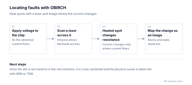
How it works
A constant voltage is applied to the chip while a focused laser scans across it. The beam warms the spot it hits slightly, which changes the resistance of any conductor or current path there. Only where current is flowing does this produce a measurable change in the supply current, so an image of current change against beam position highlights the abnormal path.
Infrared lasers with wavelengths around 1.3 µm pass through silicon. This allows observation from the backside of the chip instead of through the stack of metal layers on the front, which on modern devices blocks the view of the transistors.
Where it fits in failure analysis
OBIRCH is strong at finding metal shorts, voids in interconnects, gate-insulator leakage and spots of abnormal resistance. It is used alongside emission microscopy (EMMI), which detects faint light emitted at defect sites, and lock-in thermography, which detects heat. Each method sees different defects, so analysts often combine them.
Once these techniques narrow the fault to an area a few micrometres across, the site is cross-sectioned, usually with a focused ion beam, and examined with SEM or TEM to identify the physical cause. This sequence of electrical localisation followed by physical analysis is the standard failure-analysis flow.
Japanese companies involved
- Hamamatsu Photonics makes failure-analysis systems that combine emission microscopy with laser-scanning analysis such as OBIRCH, including backside observation through silicon.
- Hamamatsu Photonics · Failure analysis, process monitoring and static elimination equipment
FAQ
How does OBIRCH differ from emission microscopy?
Emission microscopy detects photons given off where carriers recombine or are accelerated by strong fields. OBIRCH detects resistance change caused by laser heating, so it can find faults that emit no light, such as metal-to-metal shorts or resistive vias. Using both increases the chance of locating a defect.
Why is analysis done from the backside of the chip?
Modern chips have many metal layers above the transistors that block light. Silicon is transparent to infrared, so imaging and laser scanning through a thinned substrate from the back reaches the transistors and lower layers without interference from the wiring.
Related pages
- Failure Analysis (FA)
- Leakage Current
- Scanning Electron Microscope (SEM)
- Void (Packaging Defect)
- Electromigration (EM)
- Focused Ion Beam (FIB)
- Failure analysis equipment
- Hamamatsu Photonics Dual PHEMOS®-X C16506-01
- Hamamatsu Photonics iPHEMOS®-DDX C18040-11
- Hamamatsu Photonics iPHEMOS-MPX C10506-07-06
- Hamamatsu Photonics PHEMOS-X emission microscope C15765-01
Sources
Last updated: November 13, 2026