Cross Contamination
Cross contamination is contamination in which material used in one process or product is carried into another through equipment, wafer carriers, people, air or shared chemicals. Plain contamination covers any unwanted substance; cross contamination stresses that it came from somewhere else. In chipmaking it matters most for metals that can change device behaviour.
Also called: cross-contamination
Diagram
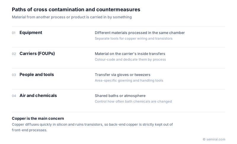
Copper and front-end segregation
The biggest concern is metals from back-end-of-line (BEOL) wiring, especially copper, reaching the front-end-of-line (FEOL) tools where transistors are built. Copper diffuses very quickly in silicon and creates energy levels in the band gap that increase leakage current and shorten carrier lifetime, so even tiny amounts are harmful.
Fabs therefore separate tools and front-opening unified pods (FOUPs) into copper and non-copper groups, mark carriers by colour or identifier, and use the manufacturing execution system to block copper-exposed wafers from entering front-end tools. Metal on the wafer backside and bevel can also be carried along, so backside and bevel cleaning is used.
Contamination inside tools
It also happens inside a single tool. In an ion implanter, a species implanted earlier can coat the beamline walls and be sputtered onto later wafers. In wet cleaning, chemicals that cleaned dirty wafers can carry contamination to the next batch, which is addressed by changing baths regularly or by single-wafer cleaning. Outgassing from resists or materials can contaminate other wafers or optics.
The basic countermeasures are separating contamination sources, dedicating tools and carriers, controlling process order, and monitoring contamination regularly.
Japanese companies involved
- Nissin Ion Equipment makes ion implanters, a tool type where cross contamination between implanted species must be managed.
- SCREEN Holdings and Tokyo Electron build cleaning systems, including single-wafer tools that reduce carry-over between wafers.
- Nissin Ion Equipment · Ion implanters
- SCREEN Holdings · Wafer cleaning, coat/develop and inspection equipment
- Tokyo Electron (TEL) · Coat/develop, etch and deposition equipment
FAQ
Why are fabs so strict about copper?
Copper moves through silicon quickly even at moderate temperatures and creates deep-level traps. A trace reaching the transistor region can raise leakage and reduce yield across a whole lot, so fabs treat copper-touched wafers and carriers as a separate class.
Can people cause cross contamination?
Yes. Gloves, tweezers and other handling tools can transfer material between areas. Fabs control this with area-specific gowning, dedicated handling tools and largely automated wafer transport, which also reduces particle generation.
Related pages
Sources
Last updated: November 2, 2026