Lift-off
Lift-off is a patterning method in which a resist pattern is made first, a film is deposited over the whole wafer, and the resist is then dissolved so that the film sitting on it comes away. Only the film that touched the bare substrate remains, so a pattern is formed without any etching step.
Also called: lift-off process, lift-off patterning
Diagram
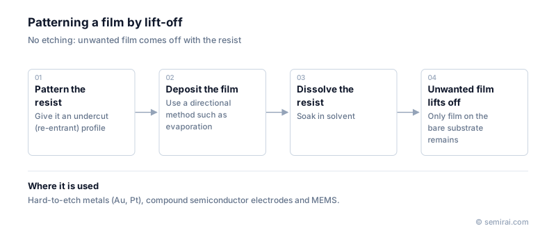
How lift-off works
The process has three steps. First, resist is coated, exposed and developed so that it is removed only where the film should stay. Second, a metal or other film is deposited over everything. Third, the wafer is soaked in a solvent or stripper, which dissolves the resist and carries away the film on top of it. This is the reverse order of conventional patterning, where the film is deposited first and then etched through a resist mask.
Clean lift-off depends on the film on the resist and the film on the substrate being separated at the pattern edge. If they are joined along the sidewall, the stripper cannot reach the resist and the film tears, leaving ragged edges. Engineers therefore give the resist a re-entrant (undercut) profile that overhangs at the top, or use a bilayer resist whose lower layer dissolves faster and forms a ledge. Electron-beam evaporation suits lift-off because atoms travel in straight lines and barely coat the shadowed sidewall; sputtering, which wraps around edges, is a poor match.
Where lift-off is used and its limits
Lift-off is chosen for metals that are hard to etch, such as gold and platinum, and when etching would damage the layer underneath. Typical uses are electrodes on compound semiconductor devices made from GaAs or GaN, gate electrodes of high-electron-mobility transistors (HEMTs), MEMS, optical devices and research prototypes.
The method has drawbacks at scale. Flakes of removed film can redeposit on the wafer, resist residue (scum) can stop the film from sticking, and burrs can remain at pattern edges. These limit yield and fine-pitch capability, so advanced silicon logic wiring is made with damascene processing or etching instead.
Japanese companies involved
- ULVAC makes vacuum deposition equipment, including evaporation systems of the kind used to deposit metal films for lift-off.
- Tokyo Electron and SCREEN Holdings build the coater/developer tracks that form the resist patterns before deposition.
- ULVAC · Vacuum deposition (sputtering) equipment and vacuum pumps
- Tokyo Electron (TEL) · Coat/develop, etch and deposition equipment
- SCREEN Holdings · Wafer cleaning, coat/develop and inspection equipment
FAQ
How is lift-off different from etching?
With etching, the film is deposited over the whole wafer and the unwanted parts are removed through a resist mask by chemicals or plasma. With lift-off, the resist pattern comes first and the unwanted film is removed together with the resist, so the film itself is never etched and the underlying layer is not exposed to etch chemistry.
Why does the resist need an undercut profile?
An overhanging top edge casts a shadow, so the deposited film does not coat the resist sidewall. That break lets the stripper reach the resist and lets the top film separate cleanly. Without it the film can bridge the edge, resist removal stalls, and torn film leaves burrs or 'wings' along the pattern.
Related pages
Sources
Last updated: November 2, 2026