EUV (Extreme Ultraviolet)
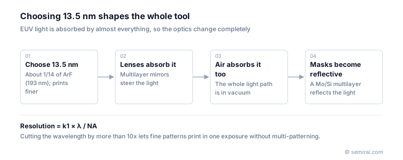
EUV (extreme ultraviolet) is light with a wavelength of 13.5 nm, used as the exposure light in lithography for the finest patterns of leading-edge chips at 7 nm-class nodes and below. Its wavelength is about one fourteenth of the 193 nm ArF laser, but because EUV is absorbed by almost every material, the entire optical path must use mirrors in vacuum.
Also called: EUV lithography, EUVL, extreme ultraviolet lithography
Diagram
How EUV light is made and guided
No laser emits 13.5 nm light directly. Production EUV sources use laser-produced plasma: tiny droplets of molten tin are hit by a pre-pulse that flattens them and then by a powerful CO₂ laser pulse, turning the tin into a hot plasma that emits EUV. This happens tens of thousands of times per second, and a collector mirror gathers the light.
Air and glass both absorb EUV, so the light travels in vacuum and is guided by mirrors coated with dozens of alternating molybdenum and silicon layers. Each mirror reflects only around two thirds of the light, so after many reflections only a small fraction reaches the wafer, which is why source power is a constant engineering focus. The mask is reflective as well.
Why chipmakers adopted it
Before EUV, the finest layers were printed with ArF immersion and multi-patterning, splitting one layer into two, three or four exposure and etch steps. Each extra step adds cost, cycle time and overlay error. EUV prints many of those layers in a single exposure, simplifies design rules and reduces process steps.
EUV is used in production for the critical layers of advanced logic and DRAM, while DUV continues to print the less demanding layers. Its main remaining challenges are stochastic defects caused by the small number of photons, source power and uptime, and pellicles that can withstand the heat.
Japanese companies involved
- Lasertec makes actinic inspection systems that inspect EUV mask blanks and masks using light at the EUV wavelength.
- HOYA and AGC make EUV mask blanks, Mitsui Chemicals makes EUV pellicles, and JSR and Tokyo Ohka Kogyo (TOK) make EUV resists.
- Rapidus has installed EUV scanners at its pilot line in Chitose, Hokkaido, for its planned 2 nm logic production.
- HOYA · Mask blanks (including EUV) and photomasks
- AGC · EUV mask blanks and glass materials
- Mitsui Chemicals · EUV pellicles and wafer protection tapes
- JSR · Photoresists and semiconductor materials
- Tokyo Ohka Kogyo (TOK) · Photoresists and high-purity process chemicals
- Rapidus · Leading-edge logic foundry (2 nm, in development)
- Lasertec · EUV mask and mask blank inspection
FAQ
What is the difference between EUV and DUV?
DUV uses 248 nm (KrF) or 193 nm (ArF) light with glass lenses, in air or with water immersion. EUV uses 13.5 nm light, which requires vacuum, multilayer mirrors and reflective masks. DUV remains the workhorse for most layers; EUV is reserved for the finest ones.
Who can build EUV scanners?
Only ASML in the Netherlands builds EUV scanners for volume production. It relies on ZEISS for the mirror optics and on a large supply chain for the light source, masks, pellicles, resists and inspection.
Why 13.5 nm and not another wavelength?
Molybdenum-silicon multilayer mirrors reflect best around 13.5 nm, and tin plasma emits strongly at that wavelength. The match between an efficient source and a practical mirror made 13.5 nm the industry choice.
Comparisons
Related pages
Sources
Last updated: November 2, 2026