Trench MOSFET
A trench MOSFET is a power MOSFET in which the gate is built inside a narrow trench etched into the silicon, so the channel runs vertically along the trench wall instead of along the surface. More cells fit into the same area, which lowers on-resistance.
Also called: trench-gate MOSFET, UMOS
Diagram
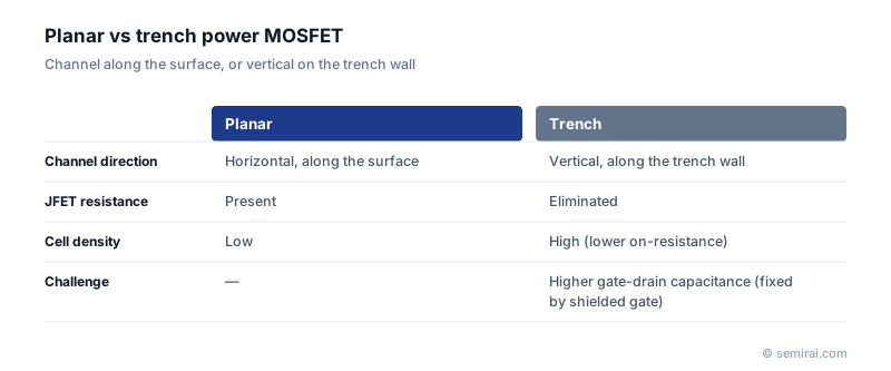
Trench vs planar structure
In a planar power MOSFET the gate lies flat on the surface. Current flows through the surface channel and then passes down between two neighbouring p-type body regions. This narrow neck adds what is called JFET resistance, and the cell pitch cannot shrink much without making it worse.
In a trench MOSFET the channel stands vertically on the trench sidewall and current flows straight down into the drift layer, so the JFET region disappears. Cells can also be packed much more densely. Together these effects cut on-resistance sharply, which is why trench designs have become the mainstream for low-voltage power MOSFETs used in DC-DC converters, motor drives and battery protection.
Design challenges
The bottom of the trench faces the drain, so the gate-drain capacitance (Cgd, also called reverse transfer or Miller capacitance) tends to be larger. That slows switching and increases gate-drive loss. Common countermeasures are a thick oxide at the trench bottom and the shielded-gate (split-gate) structure, in which a field plate connected to the source sits under the gate and screens it from the drain.
Trench gates are also used in SiC MOSFETs, but SiC's high breakdown field puts a strong electric field on the gate oxide at the trench bottom, which threatens long-term reliability. SiC trench devices therefore add p-type shielding regions or other structures to relieve that field, making the design more demanding than in silicon.
Japanese companies involved
- ROHM makes trench-gate SiC MOSFETs as well as silicon trench power MOSFETs.
- Toshiba Electronic Devices & Storage makes low-voltage trench power MOSFETs (marketed as its U-MOS series).
- Toshiba Electronic Devices & Storage · Power MOSFETs, IGBTs and discrete semiconductors
- ROHM · SiC and silicon power devices, analog ICs
FAQ
Why are high-voltage silicon MOSFETs often not trench types?
At high voltage most of the on-resistance sits in the thick drift layer, not in the channel or JFET region, so the benefit of a trench is small. High-voltage silicon devices instead use super-junction structures to lower drift resistance.
What is a shielded-gate trench MOSFET?
It places a second electrode, tied to the source, deep in the trench below the gate. This electrode screens the gate from the drain, reducing gate-drain capacitance, and also helps deplete the drift region so it can be doped more heavily for lower on-resistance.
Related pages
- MOSFET (Metal-Oxide-Semiconductor Field-Effect Transistor)
- Power Semiconductor
- Super Junction MOSFET
- SiC MOSFET (Silicon Carbide MOSFET)
- Breakdown Voltage
- Etching
- Wide Bandgap Semiconductor (WBG)
- Body Diode
- Power semiconductor manufacturing equipment
- Advantest EXAVIS
- Advantest MT100 / MT200
- Hitachi High-Tech M-600 / 6000 series
Sources
Power semiconductors terms
Last updated: November 2, 2026